Inner layer 1
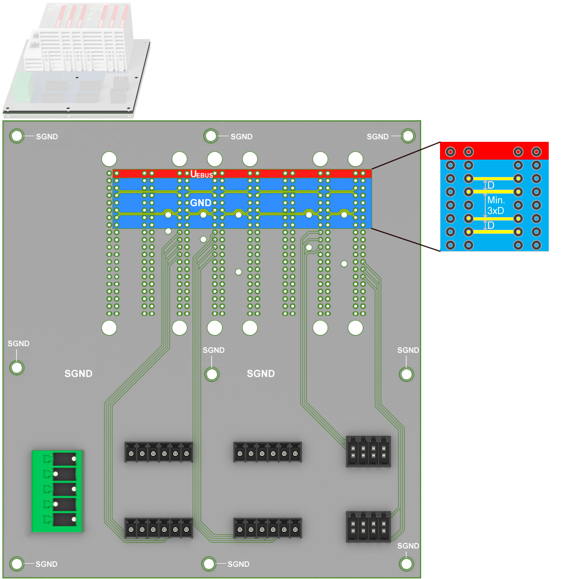
- The E-bus traces have to be routed in inner layers, in order to allow complete covering of the differential pairs with copper (GND net) from both sides of the PCB.
- On the E-bus TX and RX routing layer free space between the signals shall be filled with copper connected to GND.
- Impedance and Routing
- The differential impedance of the LVDS traces shall be 100Ω.
- Width and spacing of the differential signal are depending on the concrete layer stack up and have to be calculated individually.
- The differential signals should be routed as edge coupled traces.
- The distance between the differential pairs should be three times larger than their inner distance (see Figure above).
- Differential pairs should be routed without Vias (vertical interconnect access), in order to avoid impedance jumps.
- Maximum values for uncoupled trace and overall trace length can be found in the specification for LVDS signals ANSI/TIA/EIA-644 "Electrical Characteristics of Low Voltage Differential Signaling (LVDS)".
- It is recommended to route SGND as an area.
Physical Communication Layer
The EtherCAT plug-in modules use the E-bus for backplane communication.
The E-bus physical layer uses Low Voltage Differential Signaling (LVDS) according to the ANSI/TIA/EIA-644 „Electrical Characteristics of Low Voltage Differential Signaling (LVDS) Interface Circuits” standard.
The E-bus has a data rate of 100 Mbit/s to accomplish the Fast Ethernet data rate.