Top layer
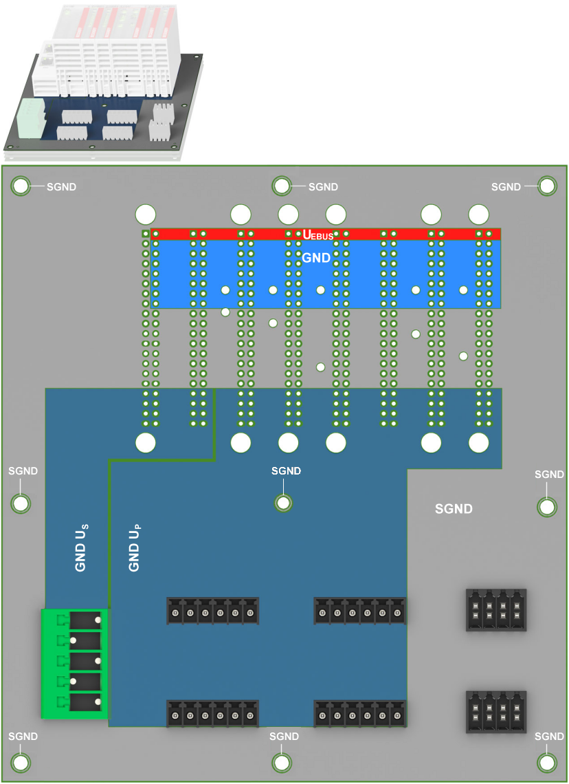
- Keep 0 V Us power supply as close as possible to the coupler in order to avoid unnecessary antennas.
- 0 V Us/Up and 24 V Us/Up should be routed at different layers.
- The SGND shield ground pins may be connected and routed on the top layer.
- SGND connection to the mounting plate shall be implemented as metal bolts building a direct connection between signal distribution board and mounting plate (see chapter SGND Connection). The copper rings around the holes are connected to SGND.
- It is recommended to route the signals SGND, 0 V Us/Up and 24 V Us/Up as an area.
 | Layout for Up power supply In the figure above, the areas for the Up supply are shown as an example. The actual layout must be adapted to the respective application. |